Saturday 31 October 2015

WEEK 7(FYP2)- ETCHING THE NEW CIRCUIT USE ON THIS PROJECT

Objective:


1) To etching the new circuit at PCB board use on this project.
2) To replace old circuit into new circuit.
3) To make the complete circuit more compact and to save the space.


Analysis/Discussion:


During week 7, this project  is 80% done basically. I founded, the hardware prototype of this project is so huge and not nicely to look because the circuit at PCB board are divided into 2 which causes a huge use of space. The presentation day of FYP 2 at week 14 and the time is still long. So, I make decision to do a new circuit at PCB board. The 2 circuit will be compile together into one circuit at PCB board.

The etching method for the circuit are also same with old circuit. I only to follow the etching method step-by-step until end. After finished etching the circuit next step is to wiring all the circuit together with all component are use and the connection must be right. After that, the complete circuit was troubleshoot and the result is very positive where all the devices are running smoothly. 

Figure 1: New circuit layout


Figure 2 : The circuit after iron at PCB board

Figure 3 : Etching the circuit

Figure 4 : The circuit after etching


Conclusion:


Finally, the complete circuit for this project was done. The circuit look so nicely and so compact compare with old circuit. Next week is to focus build the hardware prototype for this project. 

Saturday 24 October 2015

WEEK 6(FYP2)- BUILD THE HARDWARE PROTOTYPE FOR THIS PROJECT


Objective:

1) To build the hardware prototype for this project.
2) To measure the correct dimension size for the hardware prototype.         


Analysis/Discussion:

During week 6 basically measure the dimension of the all circuit to build the hardware prototype. Then to cut the prospect according to the size of the measured to build the hardware prototype.The dimension that use to build the hardware prototype for this project about the 20 cm wide x 24 cm length x 11 cm height.  After that, glue all prospect that cut by using the glue gun.


Figure 1 : process cut the prospect


Conclusion: 

Finally, the hardware prototype for this project is already done. 

Friday 16 October 2015

WEEK 5(FYP2)- LIST THE ITEM TO BUILD HARDWARE PROTOTYPE FOR THIS PROJECT


Objective:

 1) To list the items that use for build hardware prototype in this project.
 2) To buy the items that use for build the hardware prototype in this project.


Analysis/Discussion:

During week 5 basically list the items that use to build the hardware prototype such as the important items is prospect, cordless drill, glue gun, and others. The items listed was re-check to avoid the wrong items and to reduce the cost. The items listed was buy at hardware shop, Mr. DIY shop and signboard shop. I've no problem to buy all items that use because all items is already has at shop.

Conclusion:


Finally, after finish listed and buy the items that need to build the hardware prototype of this project next steps is to cut and combine the pieces of prospect that use to build the hardware prototype

Friday 9 October 2015

WEEK 4 (FYP2) - ETCHING THE CIRCUIT ARE USE ON THIS PROJECT


Objective:

1) To etching the circuit that use using PCB board


Analysis/Discussion:

During week 7 basically doing the etching for the circuit that use in this project by followed the step or procedure that studies before during making the diploma and advice by friend that has knowledge about the etching process.

The etching method are:


Step 1: Finalize Circuit Design

Everything starts with the circuit design. Without a circuit there is no need for a PCB. Before student even begins to lay out PCB, student must have a complete and accurate schematic diagram. In today‘s world of modern computing, the circuit design is capture directly in a schematic. Schematic design can be obtain from source such internet and books. Some of the schematic design student obtains from lecturer and intensive class student attend.

Step 2: PCB Layout Design

In general “capturing the schematic” is the process by which each component is drowns electronically and is interconnected with each other. Once the schematic is complete its time to draw the physical outline of each of the components. These outlines are what are placed on the PCB in copper to allow the components to be soldered to the printed wiring board.

Figure 1 : PCB layout design


Step 3: Ironing the Layout Method

Put a white paper on the OHP sheet and start ironing. The heat applied by the electric iron causes theink of the traces on the OHP sheet to stick on the copper plate exactly in the same way it is printed on the OHP sheet. This means that the copper sheet will now have the layout of the PCB printed on it. Allow the PCB plate to cool down and slowly remove the OHP sheet. Since it is manual process it may happen that the layout doesn’t comes properly on PCB or some of the tracks are broken in between. Use the permanent marker and complete the track properly.

 
Figure 1: Ironing the layout method

Step 4: Etching and Drill, 

Etching process is important to make sure all connection will connect between components. First step of etching is stick the design at PCB board and it should paste all of the carbon because it the way of current flow between component. Next, by using etching liquid the process is erodible the cooper layer until left only copper line at circuit. Then, clean up circuit layer until look shiny and start process of drill a hole of pin component. 


Figure 2 : Etching the PCB board


Step 5: Solder and Testing

Next, put the components in the correct holes and solder them. Lastly, after all this process it should be testing to check the connection of circuit is correct or wrong and must be in good condition.

Figure 3 : Solder the component into PCB board

Figure 4 : All the circuit and component are connected each other with right connection


Conclusion: 


Finally, after finish etching the circuit use in this project next steps is to wiring all the circuit together with right connection. The circuit was troubleshoot and several devices was not working properly. After the troubleshooting process, the devices can be working properly. So, hardware prototype of this project can be start to build. 

Saturday 3 October 2015

WEEK 3(FYP2) - PREPARE AND BUY THE LIST OF COMPONENT FOR THE PROJECT


Objective:


1) Buy the component use for this project.

2) To calculate the budget and cost for this project.


Analysis/Discussion:


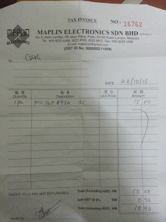
         During week 3, basically buy the listed component that want to use in this project such as the important component. Then, to avoid the actual cost and budgets for this project is to expensive when buy the component as we know because the price of the electronic component increase and if late to buy the cost for this project will increase. The component that listed such as the PCB, Keypad, LCD and others has already in stock and can buy. The total price is listed in the receipt that attach.

Figure 1

Figure 2

Figure 3

Figure 4


Conclusion: 


        Finally, the important component has been buy at Jalan Pasar and the cost not too expensive but has certain component the price has increase and all important components gets then next for next week it can be used to test the circuit for this project.