Friday 18 December 2015

WEEK 14 (FYP2) - INDUSTRIAL DAY


Objective: 

1) To present the project that develop
2) To demo the project


Analysis/Discussion:

During week 14, basically the presentation day to the project  that develop at assessors to give mark and give the feedback about this project. The assessors that decided for this project are Madam Siti Zaiummi binti Mohd Zawawi and Madam Salmi binti Idin. Firstly, I present my project to assessors based on my poster. My project are totally showed from introduction until conclusion at the poster. So, I only explain more details about my project with full confident and  make the assessors understand about my project. After finished the explanation about my project, the assessors ask me some question regarding my poster. I answering the question smoothly until they satisfied with my answer. Lastly, I bring the assessors to outside the hall because I want to demo my project to them. The demo is to prove my project whether function or not and my project totally function. The feedback from assessors are positive after the demo.


During presentation to the assessors


After finished the presentation

Conclusion:

Finally, the Industrial Day/ Presentation Day was successfully done without has any problem. The system of my project working properly and the project successful to finished. So, for the next step is to submit my final year project full report with hardcover to my supervisor and university library.

Saturday 12 December 2015

WEEK 13 (FYP2) - MAKING THE PREPARATION FOR THE INDUSTRIAL DAY AND DESIGN POSTER


Objective:

1) To repair the draft for final project report  

2) To design the poster for industrial day. 


Analysis/Discussion:

During week 13, basically repair  the final report draft for this project after referred from supervisor. Then, design the poster for presentation day about the project develop. After that, make the final preparation for presentation day by test the hardware prototype and select the specific information to put in the poster.

This week the draft report was repair and finish write then, the poster was design successfully by add the important information about this project and was printed A1 size ready to present next week during presentation day. All preparation was successful and do not has any problem to prepare because by follow the gantt chart that guide the successful of this project so the work was finish during the due date without has any problem.


Figure 1: Poster Development of Bike Security System


Conclusion:

   Finally, the draft final report that write followed the correct guideline and was repair by add some suggestion from supervisor madam noor hidayah. Then, poster design was finish  and ready for presentation day next week.

Saturday 5 December 2015

WEEK 12 (FYP2) - TOUCH UP THE FINAL REPORT DRAFT 


Objective:

1) To touch up the final report draft.


Analysis/Discussion:

During week 12, basically write the draft report. The draft report was cover from chapter 4 and chapter 5 only because chapter 1, chapter 2 and chapter 3 was completed in final year project 1 last semester. By refer the proposal report was finish from Final Years project 1 and the result that record for this project all information was collect and put into the draft report. The draft report making more easy and do not has any problem by follow the guideline how to write the final report.


Conclusion:

After complete the draft report for chapter 4 and chapter 5, the draft report was sent to madam noor hidayah binti mohd yunus to checking either it correct or not.

Saturday 28 November 2015

WEEK 11 (FYP2) - FINAL YEAR PROJECT BRIEFING #2 AND TROUBLESHOOT THE PROJECT.

Objective:

1) To attend final year project briefing #2.
2) To troubleshoot the project.


Analysis/Discussion:

Basically on week 11, has briefing #2 for final year project. During final year project briefing inform the guideline during the industrial day and also the guideline how to making the poster for the project develop. Then, the lecturer remind to get ready for the industrial day.


Figure 1: The memo for final year project briefing


Besides that, the process of combining the hardware prototype to the bike is continued. The problem of previous work is solved by using troubleshooting method with the guide of some friends.   


Conclusion:

Finally, the objectives of development of bike security system are achieved where to make the bike will not easily to START, to get the people surrounding alert when the bike try to be stolen and to designed and develop the hardware security system of the proposed system. 

Friday 20 November 2015

WEEK 10 (FYP2)- WIRING THE HARDWARE PROTOTYPE TO THE BIKE


Objective:

1) To wiring the hardware prototype to the bike.

Analysis/Discussion:

During week 10 basically after doing some research about bike wiring, I'm doing the wiring connection between my hardware prototype into my bike. After that, test and troubleshoot the wiring connection if function or not.While during the wiring connection, there were some problem occurred such as integrated circuit (IC) PIC 16F877A burned and the bike still can be function even though the key in password is wrong.  

Figure 1

Figure 2

Figure 3


Conclusion:

The process of combining hardware prototype to the bike is not easy as I thought where some problem occurred during the process. The process continued until week 11.

Friday 13 November 2015

WEEK 9(FYP2)- STUDY ABOUT BIKE WIRING.


Objective:

1) To study about bike wiring diagram.


Analysis/Discussion:

Figure 1: Bike wiring diagram.(Reference 1)

Figure 2: Bike wiring diagram.(Reference2)

Figure 3: Bike wiring diagram.(Reference 3)
For this week, The output of my project is bike. So I must study about bike wiring connection. I can choose to use dc motor replace the bike as a output for this project. But I think I want to try challenge myself to connect my project into the bike. Many resources to refer the wiring connection of bike at the internet. Figure above as an example of bike wiring connection. Besides that, I also refer or ask my friends to give their opinion about bike wiring system to me.  


Conclusion:


Finally after research about bike wiring system, I more confident to connect my circuit into the bike because wiring system of the bike are not difficult as we are expected.

Friday 6 November 2015

WEEK 8(FYP2)- FINAL YEAR PROJECT  2 BRIEFING FOR 1ST TIME


Objective:


1) To attend Final Year Project 2 briefing.
2) To build the new hardware prototype for this project.


Analysis/Discussion:


    During week 8 basically has attend the Final Year Project 2 briefing then continue by doing the new hardware prototype for this project. I only to buy a prospect item at signboard shop for the new hardware prototype for this project. The other items such as cordless drill, glue gun, and others have already. So, the new hardware prototype for this project can be build by measure the dimension of the complete circuit at first step. Then, to cut the prospect according to the size of the measured to build the new hardware prototype.The dimension that use to build the new hardware prototype for this project about the 20 cm wide x 24 cm length x 11 cm height.  After that, glue all prospect that cut become a rectangular box by using the glue gun. Then, the complete circuit will be located at the base surface of the box while only keypad, led and lcd are located at the upper surface of the box to display them.
Figure 1 : The hardware prototype for this project


 Conclusion:


         Finally,the new hardware prototype for this project was built. The new hardware prototype look very nicely, small and so compact compare with the old hardware prototype. So, the hardware prototype can be connected to the motorcycle after this. 


Saturday 31 October 2015

WEEK 7(FYP2)- ETCHING THE NEW CIRCUIT USE ON THIS PROJECT

Objective:


1) To etching the new circuit at PCB board use on this project.
2) To replace old circuit into new circuit.
3) To make the complete circuit more compact and to save the space.


Analysis/Discussion:


During week 7, this project  is 80% done basically. I founded, the hardware prototype of this project is so huge and not nicely to look because the circuit at PCB board are divided into 2 which causes a huge use of space. The presentation day of FYP 2 at week 14 and the time is still long. So, I make decision to do a new circuit at PCB board. The 2 circuit will be compile together into one circuit at PCB board.

The etching method for the circuit are also same with old circuit. I only to follow the etching method step-by-step until end. After finished etching the circuit next step is to wiring all the circuit together with all component are use and the connection must be right. After that, the complete circuit was troubleshoot and the result is very positive where all the devices are running smoothly. 

Figure 1: New circuit layout


Figure 2 : The circuit after iron at PCB board

Figure 3 : Etching the circuit

Figure 4 : The circuit after etching


Conclusion:


Finally, the complete circuit for this project was done. The circuit look so nicely and so compact compare with old circuit. Next week is to focus build the hardware prototype for this project. 

Saturday 24 October 2015

WEEK 6(FYP2)- BUILD THE HARDWARE PROTOTYPE FOR THIS PROJECT


Objective:

1) To build the hardware prototype for this project.
2) To measure the correct dimension size for the hardware prototype.         


Analysis/Discussion:

During week 6 basically measure the dimension of the all circuit to build the hardware prototype. Then to cut the prospect according to the size of the measured to build the hardware prototype.The dimension that use to build the hardware prototype for this project about the 20 cm wide x 24 cm length x 11 cm height.  After that, glue all prospect that cut by using the glue gun.


Figure 1 : process cut the prospect


Conclusion: 

Finally, the hardware prototype for this project is already done. 

Friday 16 October 2015

WEEK 5(FYP2)- LIST THE ITEM TO BUILD HARDWARE PROTOTYPE FOR THIS PROJECT


Objective:

 1) To list the items that use for build hardware prototype in this project.
 2) To buy the items that use for build the hardware prototype in this project.


Analysis/Discussion:

During week 5 basically list the items that use to build the hardware prototype such as the important items is prospect, cordless drill, glue gun, and others. The items listed was re-check to avoid the wrong items and to reduce the cost. The items listed was buy at hardware shop, Mr. DIY shop and signboard shop. I've no problem to buy all items that use because all items is already has at shop.

Conclusion:


Finally, after finish listed and buy the items that need to build the hardware prototype of this project next steps is to cut and combine the pieces of prospect that use to build the hardware prototype

Friday 9 October 2015

WEEK 4 (FYP2) - ETCHING THE CIRCUIT ARE USE ON THIS PROJECT


Objective:

1) To etching the circuit that use using PCB board


Analysis/Discussion:

During week 7 basically doing the etching for the circuit that use in this project by followed the step or procedure that studies before during making the diploma and advice by friend that has knowledge about the etching process.

The etching method are:


Step 1: Finalize Circuit Design

Everything starts with the circuit design. Without a circuit there is no need for a PCB. Before student even begins to lay out PCB, student must have a complete and accurate schematic diagram. In today‘s world of modern computing, the circuit design is capture directly in a schematic. Schematic design can be obtain from source such internet and books. Some of the schematic design student obtains from lecturer and intensive class student attend.

Step 2: PCB Layout Design

In general “capturing the schematic” is the process by which each component is drowns electronically and is interconnected with each other. Once the schematic is complete its time to draw the physical outline of each of the components. These outlines are what are placed on the PCB in copper to allow the components to be soldered to the printed wiring board.

Figure 1 : PCB layout design


Step 3: Ironing the Layout Method

Put a white paper on the OHP sheet and start ironing. The heat applied by the electric iron causes theink of the traces on the OHP sheet to stick on the copper plate exactly in the same way it is printed on the OHP sheet. This means that the copper sheet will now have the layout of the PCB printed on it. Allow the PCB plate to cool down and slowly remove the OHP sheet. Since it is manual process it may happen that the layout doesn’t comes properly on PCB or some of the tracks are broken in between. Use the permanent marker and complete the track properly.

 
Figure 1: Ironing the layout method

Step 4: Etching and Drill, 

Etching process is important to make sure all connection will connect between components. First step of etching is stick the design at PCB board and it should paste all of the carbon because it the way of current flow between component. Next, by using etching liquid the process is erodible the cooper layer until left only copper line at circuit. Then, clean up circuit layer until look shiny and start process of drill a hole of pin component. 


Figure 2 : Etching the PCB board


Step 5: Solder and Testing

Next, put the components in the correct holes and solder them. Lastly, after all this process it should be testing to check the connection of circuit is correct or wrong and must be in good condition.

Figure 3 : Solder the component into PCB board

Figure 4 : All the circuit and component are connected each other with right connection


Conclusion: 


Finally, after finish etching the circuit use in this project next steps is to wiring all the circuit together with right connection. The circuit was troubleshoot and several devices was not working properly. After the troubleshooting process, the devices can be working properly. So, hardware prototype of this project can be start to build. 

Saturday 3 October 2015

WEEK 3(FYP2) - PREPARE AND BUY THE LIST OF COMPONENT FOR THE PROJECT


Objective:


1) Buy the component use for this project.

2) To calculate the budget and cost for this project.


Analysis/Discussion:


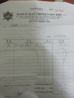
         During week 3, basically buy the listed component that want to use in this project such as the important component. Then, to avoid the actual cost and budgets for this project is to expensive when buy the component as we know because the price of the electronic component increase and if late to buy the cost for this project will increase. The component that listed such as the PCB, Keypad, LCD and others has already in stock and can buy. The total price is listed in the receipt that attach.

Figure 1

Figure 2

Figure 3

Figure 4


Conclusion: 


        Finally, the important component has been buy at Jalan Pasar and the cost not too expensive but has certain component the price has increase and all important components gets then next for next week it can be used to test the circuit for this project.


Saturday 26 September 2015

WEEK 2 (FYP 2) -PREPARE THE LIST OF THE COMPONENT FOR THE PROJECT

Objective:


1) To list the component that use in this project.


2) To prepare the budget.


Analysis/Discussion:


         During week 2 basically list the component that want to use in this project such as the important component.The component that listed such as the PCB, Keypad, Relay, PIC, LCD and others. After that, re-check the component that use with the component that list in the proposal to avoid the wrong component use. Then, to prepare the actual budgets for this project by searching the price of the component by website and survey the price from shop at Jalan Pasar the price for component is different between website and shop at Jalan Pasar.


Conclusion: 


       Finally, after finish listed the component that want to use in this project and survey the actual price by looking at website and shop at Jalan Pasar after calculate the time taken to gets the component.I decide to buys at Jalan Pasar because fastest to gets the important component to test the circuit. 

Saturday 19 September 2015

WEEK 1(FYP 2): THE FYP 2 BEGINS

Objective:


To introduce the second semester of the final year project.


Analysis/discussion:


        The first week of the 7th semester has just begin. At the end of the previous semester, I have successfully submitted the proposal report. Now that the proposal has been approved and I can start to make the product.


Conclusion: 

The project of Development of Bike Security System has been started.


Sunday 17 May 2015

WEEK 14- SUBMITTED FINAL PROPOSAL REPORT

Objective: 

To finish and submit the final proposal report.

Analysis/Discussion:

This is the last week for me to finish up my final proposal report.The last day to submit is on friday. Before I submitted my final proposal report, my supervisor want me to correct my literature review and my methodology. For literature review, Madam Hidayah ask me to add more related history as a reference of my project. Besides that, for methodology Madam Hidayah also told me my methodology have block diagram and flow chart but no description about block diagram and flow chart. So, I must explain the block diagram and flow chart step by step.  

Conclusion:  

By Friday,15/5/2015, I have submitted my final proposal report(chapter 1,2 and 3) to Madam Hidayah.

Sunday 10 May 2015

WEEK 13 - PROPOSAL REPORT DRAFT

Objective: 

To finish and submit the proposal report draft.

Analysis/Discussion:

This is the last week for me to finish up my proposal report draft because my supervisor want to check it before final proposal report submitted. The last day to submit is on Friday. This week I need finish up the small parts in the report. The sections left are the:-
  1. Abstract
  2. Table of Content
  3. Conclusion
  4. Formatting the report

Conclusion:  

By Friday,8/5/2015, I have submitted my proposal report draft to Madam Hidayah.

Saturday 2 May 2015

WEEK 12 - PROPOSAL REPORT

Objective: 

To finalize the proposal report.

Analysis/Discussion:

This week I need to finalize my proposal report. The proposal report is almost 70% finished. But, this week I am a little bit busy with other reports I have only a little time to work on the proposal report. Fortunately, the proposal report due is next 2 week.  

Conclusion:

 A very small progress this week. I need to make it up in week 13.

Thursday 30 April 2015

WEEK 11 - FYP 1 PRESENTATION

Objective:

Briefing about the Final Year Project 1 presentation.


Analysis/Discussion:


The Final Year Project 1 presentation took place in the Dewan Gemilang, Unikl British Malaysian Institute (BMI) on 22nd of April 2015. The presentation started at 2:00 in the evening. I was assigned to two assessors from the FYP committee whom are lecturers from the Communication Section. The assessors are Sir Saiful Yusri Mohd Yassin and Madam Dr. Alipah Pawi.


The first assessor is Sir Saiful Yusri. I presented my proposal project presentation to him. He listened through the presentation until the question and answer (Q&A) session which he asked a few questions. Fortunately, I answered all his question. In the end of the first presentation, he suggested that I should clearly state my methodology.


The second presentation with Madam Dr.Alipah also went well. Again, I successfully answered her question during the Q&A session. In the end of the second presentation, she suggested that I should clearly state my work plan at the gantt chart. She ask me to refer my supervisor about the gantt chart.

Conclusion:

Though the presentation has ended and went with flying colours, I still need to finish up and I also need to correct a few parts in the proposal report.